How to Design Your Own PCB Explained Step Circuit Diagram Create Gerber Files in KiCad. From the PCB Editor in KiCad you can create Gerber files by going to the File menu and selecting Plot… A window will appear. Click on the Plot button to create the Gerber files. To create Drill files, click on Generate Drill Files… to open the Drill File dialog. Then click the button Generate Drill File. Learn how to design your own PCB step-by-step, from creating a schematic to building a board. Find out the best PCB design software, materials, and manufacturers for your project.
4. Design your PCB stackup. This is important to consider early on in the PCB design stage due to impedance, which refers to how much and how quickly electricity can travel down a trace. The stackup plays a role in how the mechanical engineer can design and fit the PCB into the device. 5. Define design rules and requirements.

Online PCB Design Tutorial for Beginners Circuit Diagram
Step 2: Create a Blank PCB Layout . Next you're going to create the layout where your schematic is going to come to life. Create a PcbDoc File: Open up a new PCB document in your CAD tool. Define Board Outline: Shape and dimension the board according to the needs of the project.
Learn the steps to design and make your own PCB from a circuit diagram. Find out how to use KiCad software, choose components, order PCBs, and solder them.

How to Design a Printed Circuit Board Circuit Diagram
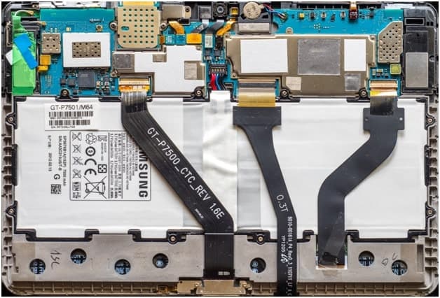
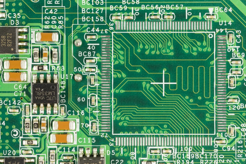
What is a PCB and Intro to PCB Design Printed circuit board (PCB) design has grown into its own specialized field within the electronics industry. PCBs play an important role in that they provide electrical interconnections between electronic components, rigid support to hold components, and a compact package that can be integrated into an end Larger circuits can be difficult to design on a single layer PCB. As design complexity increases, it gets harder to route the traces without intersecting one another. Luckily there are double, triple, and multi-layer PCBs that allow traces and planes to be routed on electrically isolated layers.
